
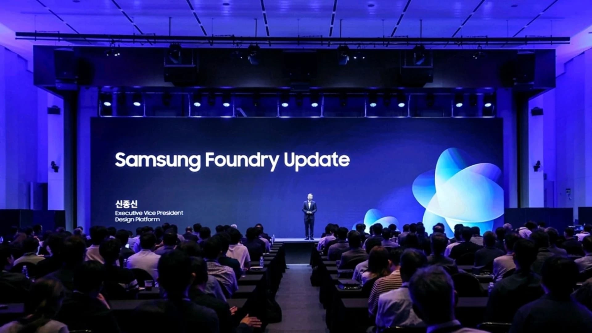
Samsung Foundry will delay full commercial use of High-NA EUV lithography until its 1nm node, A10. Park Chang-min confirmed the shift at the NGL 2026 conference in Korea, putting Samsung 1nm chip output near 2030. That single call decides which machines etch your next several Galaxy processors.
Key Takeaways
- Samsung will hold off on full commercial High-NA EUV use until its 1nm A10 node. Chips from that node should reach the market around 2030.
- The 2nm and 1.4nm nodes will run on standard 0.33 NA EUV scanners plus multi-patterning. Samsung had originally planned High-NA for both.
- Park Chang-min pointed to an unfinished supply chain of masks, pellicles, and specialty materials. Samsung is co-developing those parts with outside partners.
- Each High-NA scanner carries an estimated price of $350 million to $400 million. That figure is roughly double a standard EUV machine.
- Intel already runs High-NA layers in volume production, and ASML confirmed it in July 2026. TSMC lands near Samsung at 2029 or 2030.
Samsung Moves High-NA EUV to the A10 Node
Park Chang-min works as a Master on the Foundry Process Development Team at Samsung's Semiconductor R&D Center. He told the Next Generation Lithography and Patterning Conference that commercial High-NA use begins at A10. ZDNet Korea reported his remarks, and SamMobile covered the decision on August 11, 2026, crediting the leaker Jukan05.
Samsung will build its 2nm and 1.4nm nodes on 0.33 NA EUV scanners paired with multi-patterning. The company had intended to run High-NA on both of those nodes.
Park blamed the supporting supply chain. Masks, pellicles, and specialty materials for High-NA remain immature, and Samsung is developing them jointly with suppliers.
Price adds weight to the decision. Each High-NA scanner costs an estimated $350 million to $400 million.
Why Samsung Walked Back Its 2nm High-NA Plan
Samsung has owned High-NA hardware for more than a year. The Financial News reported that Samsung installed an EXE:5000 research tool at its Hwaseong campus in March 2025.
Buying followed quickly. The Korea Economic Daily reported in October 2025 that Samsung committed 1.1 trillion won, about $773 million, to two Twinscan EXE:5200B units. Industry sources told the outlet those tools were headed for 2nm lines building the Exynos 2600.
Read both reports next to this week's news and the picture sharpens. Samsung owns the machines and has decided against trusting them with a revenue node for another five years.
The move fits Samsung Foundry's recent behaviour. The company chased a first-mover title on 3nm gate-all-around in 2022, then spent three years repairing yields. Sitting out the opening High-NA wave reads as a lesson applied.
Key Details on Samsung's Node Roadmap and Its Rivals
Samsung already ships 2nm silicon. The Exynos 2600 entered mass production on the SF2 process in late 2025 and powers Galaxy S26 models.
ZDNet Korea, cited by TrendForce, places SF1.4 in mass production during 2029. SF1.4+ and the 1nm node follow in 2030.
Intel reached volume production first, and ASML documented it. ASML confirmed on July 15, 2026 that specific Intel 18A layers are dual-qualified on High-NA in Oregon, shipping Core Ultra Series 3 Panther Lake parts at matched yields.
TSMC has ruled High-NA out for its A14 node, per Bits&Chips. The company targets commercial insertion around 2029 or 2030, which puts it alongside Samsung.
| Foundry | First commercial High-NA node | Expected timing | Status today |
|---|---|---|---|
| Samsung | 1nm / A10 | Around 2030 | Research and pilot tools on site, 2nm and 1.4nm stay on 0.33 NA |
| Intel | Select Intel 18A layers, then 14A | Shipping now, 14A ramp in 2028 | High-volume production on qualified 18A layers, per ASML |
| TSMC | Undisclosed node after A14 | Around 2029 to 2030 | R&D tools only, A14 confirmed without High-NA |
High-NA raises numerical aperture from 0.33 to 0.55. The optics gather more light, resolve finer features, and let a fab print in one pass what previously took several.
Multi-patterning delivers the same result through extra work. Every added exposure brings another mask, more cycle time, and another chance to introduce a defect.
PRO TIP: Node names are marketing labels. Judge a chip on published transistor density and power figures rather than the nanometer badge.
What's Confirmed and What's Still Unclear About the Samsung 1nm Chip Plan
Confirmed: Park Chang-min said Samsung adopts High-NA EUV commercially at the 1nm A10 node, per ZDNet Korea and SamMobile.
Still Unclear: Samsung has issued no newsroom post or investor slide carrying that timeline.
What It Means: Treat 2030 as a working target voiced at a conference, not a locked schedule.
Confirmed: Samsung's 2nm and 1.4nm nodes will use 0.33 NA EUV with multi-patterning, according to the same reporting.
Still Unclear: Samsung has not disclosed how many extra mask layers this adds or what it does to wafer pricing.
What It Means: Expect wafer costs at 1.4nm to climb, and expect part of that to reach retail phone prices.
Confirmed: Samsung committed roughly 1.1 trillion won to two EXE:5200B scanners, per The Korea Economic Daily.
Still Unclear: Samsung never confirmed the purchase publicly, and outlets describe Park's title three different ways. Bits&Chips called him a company executive, TrendForce called him a Master and senior technology expert, and Wccftech called him a VP of technology.
What It Means: The direction holds up across sources. The specifics come from Korean media, not Samsung filings.
Confirmed: ASML stated that Intel runs High-NA layers in high-volume manufacturing on Intel 18A.
Still Unclear: No company has published a cost-per-wafer comparison between High-NA single patterning and 0.33 NA multi-patterning.
What It Means: Nobody outside these fabs can prove Samsung made the wrong call.
What Samsung's 1nm Chip Timeline Means for Your Galaxy Phone
Nothing changes for the Galaxy S26 already in your pocket. Its Exynos 2600 came off 0.33 NA tooling, and this announcement does not touch that.
The medium term is where the decision bites. Galaxy flagships through roughly 2029 will carry chips built with multi-patterning, which adds process steps to every wafer.
More steps push cost up and squeeze yield windows. Samsung Foundry absorbs part of that, and the remainder lands in a phone's bill of materials.
Does that mean your 2028 Galaxy feels slower? No. Node choice sets the ceiling on battery life and sustained performance, not the peak numbers you see in a benchmark run.
Supply is the sharper worry. Samsung needs enough good wafers to put an Exynos in every S-series unit it sells, and multi-patterning makes that arithmetic harder.
How much do you genuinely care which machine printed your processor? Most Galaxy owners care about the result, which is a phone that survives a full day. Update policy shapes ownership more directly, and our breakdown of the Samsung software update roadmap for August 2026 shows how long each model stays patched.
WARNING: Ignore any spec sheet claiming a phone uses a High-NA-built chip before 2030. No foundry has committed mobile silicon to those tools.
Frequently Asked Questions About the Samsung 1nm Chip Node
Q: When will Samsung start making 1nm chips?
A: Samsung targets mass production of its 1nm A10 node around 2030, per ZDNet Korea's report from NGL 2026. SF1.4 arrives first in 2029, with SF1.4+ and 1nm following in 2030. Samsung has published no official date of its own.
Q: Why is Samsung delaying High-NA EUV?
A: Park Chang-min said the ecosystem around the tool is not ready. Masks, pellicles, and specialty materials require further joint development with suppliers. Each scanner also costs $350 million to $400 million, so Samsung wants proof before assigning it a revenue node.
Q: Which Galaxy phones will use a Samsung 1nm chip?
A: None have been announced. A 2030 production start points to a Galaxy S-series flagship in 2030 or 2031 at the earliest. Every Galaxy launching before then uses 2nm or 1.4nm class silicon printed on 0.33 NA EUV.
Q: Is Samsung behind Intel on High-NA EUV?
A: On deployment, yes. ASML confirmed in July 2026 that Intel Foundry runs High-NA layers in high-volume manufacturing on Intel 18A. Samsung and TSMC both aim for commercial use around 2029 to 2030, so Intel holds a multi-year lead.
Q: What does High-NA EUV actually improve?
A: It lifts numerical aperture from 0.33 to 0.55, which sharpens optical resolution. Fabs print finer features in one exposure rather than several. Fewer exposures shorten cycle time and reduce the chances of introducing a defect.
What to Watch Between Now and Samsung's 1.4nm Ramp
Watch SF1.4 in 2029. Samsung's ability to hold that date on 0.33 NA multi-patterning decides whether the Samsung 1nm chip plan survives contact with reality.
Watch the second EXE:5200B as well. Any report of that scanner moving from research into a pilot line would signal an earlier High-NA move than Park described.
Software timelines matter more than lithography for the phone you own today, and our report on Galaxy S23 One UI 9 as the final major update shows how Samsung sets those clocks.
Which Galaxy are you planning to keep until 2030, and does foundry roadmap news change what you buy next? Post your model in the comments and say whether an Exynos or a Snapdragon is your preference this cycle.








Responses (0 )